¶ Order Yours Today
| Store | URL | Description | Stock Status |
|---|---|---|---|
| Official Store | store.bqvoy.com | Our Official Store, Secure Payments By Stripe, Volume Discount Available | US915MHz: Loading EU868MHz: |
¶ Introduction
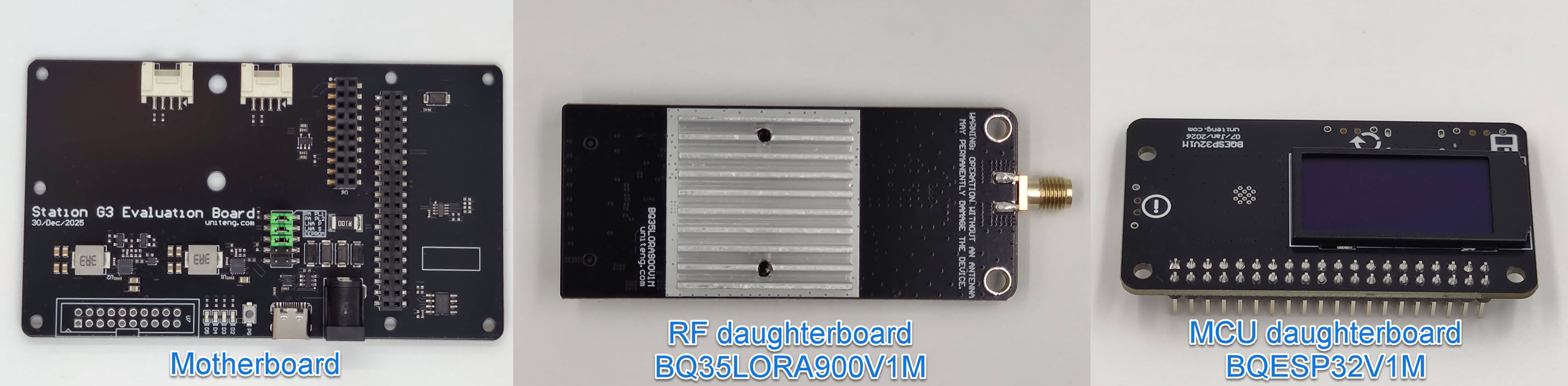
The Station G3 is a modular development board that includes a motherboard, an RF daughterboard, and an MCU daughterboard, making it possible to configure/upgrade each daughterboard individually. We believe this will help extend the lifecycle of RF designs and make it easier for more engineers to integrate Station G3 into their designs.
The MCU daughterboard socket is compatible with the standard Raspberry Pi 40-pin GPIO header definition. Experienced users can use the Raspberry Pi Zero 2W with Header as an MCU daughterboard to build their own Linux Mesh nodes.
¶ Official Order Options
¶ Order Option - ESP32S3-BQ35LORA900V1M
This configuration is fully compatible with Station G2 at the firmware level and can directly use most Station G2 firmware.
Package/lot:
- 1 x Motherboard
It employs the same Fast-Transient DC-DC for LoRa Power Amplifier technology as the Station G2, providing excellent power support to ensure the correct transmission and reception of LoRa packets. - 1 x MCU daughterboard - BQESP32V1M
This module is built using an ESP32 S3 (Flash: 16MB, PSRAM: 8MB) and a 1.3-inch OLED screen. - 1 x RF daughterboard - BQ35LORA900V1M
Supports the 850 MHz–930 MHz frequency band, featuring a up to 35 dBm PA for transmit and LNA design with dynamic gain control and impedance matching for receive.
- 1 x Lora Antenna
915Mhz Antenna for Region Option=US915Mhz
OR
868Mhz Antenna for Region Option=EU868MHz
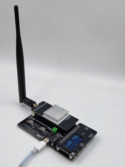
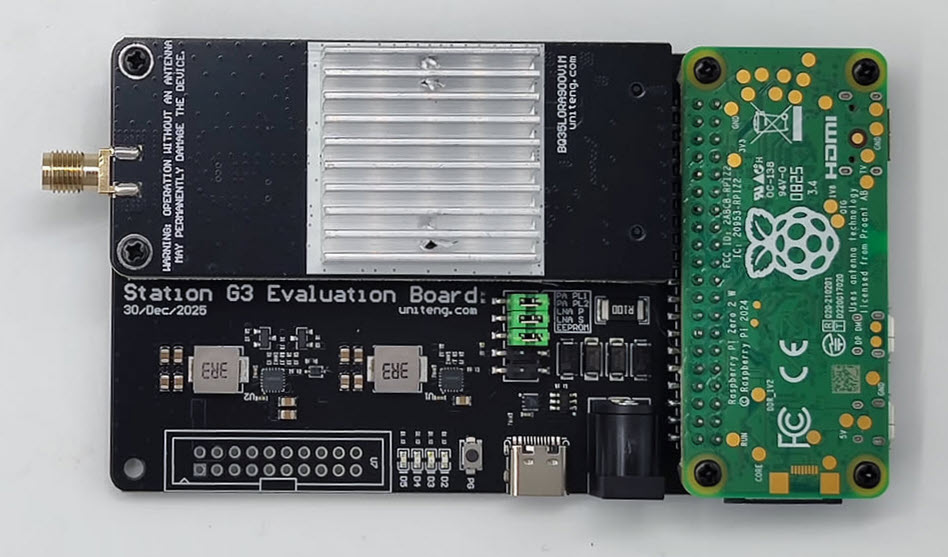
Users will receive a pre-assembled development board as shown in the image below:
Note: the USB cable is not included in the package.
¶ Quick Start Guide
¶ Safety & Compliance
WARNING: OPERATION WITHOUT AN ANTENNA MAY PERMANENTLY DAMAGE THE DEVICE.
WARNING: OPERATE ON AN INSULATED SURFACE. ENSURE PROPER INSULATION DURING OPERATION.
WHETHER USING A 15VDC USB TYPE-C PD ADAPTER OR A 9VDC–19VDC EXTERNAL POWER SUPPLY, THE MAXIMUM PEAK INPUT VOLTAGE TO THE STATION G3 MUST NOT EXCEED 19V. OTHERWISE, THE DEVICE MAY BE PERMANENTLY DAMAGED.
PLEASE FOLLOW LOCAL RF REGULATIONS TO SELECT THE APPROPRIATE PA OPERATING MODE.
¶ Step 1 – Install the Antenna
Before powering on the device, please install the antenna as shown in the picture below.
¶ Step 2 – Configure Hardware
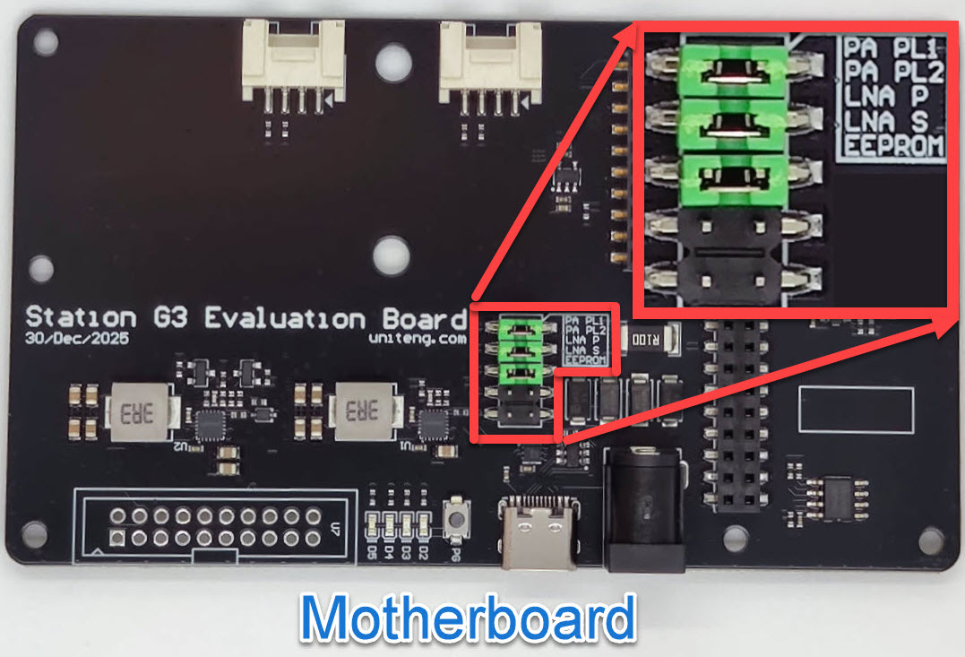
The hardware configuration of Station G3 is set via 5 jumpers located on the motherboard. In this section, we focus on the first 3 jumpers, PA PL1, PA PL2 and LNA P. The LNA S and EEPROM jumpers are reserved. By default, the 2.54mm jumpers are not installed for both LNA S and EEPROM.
¶ Power Amplifier Operating Mode Configuration Jumper PA PL1 and PA PL2.
| PA Operating Mode | PA PL1 | PA PL2 | Description |
|---|---|---|---|
| Power Level 1 | OPEN | OPEN | Default recommended setting. When the device is in the TX state, both the PA output power and the overall power consumption of the device are at their lowest levels. Minimum Power Supply Voltage Requirement: 9 VDC. |
| Power Level 2 | OPEN | SHORT | PA output power and the overall power consumption is higher than Power Level 1. Minimum Power Supply Voltage Requirement: 9 VDC. |
| Power Level 3 | SHORT | OPEN | PA output power and the overall power consumption is higher than Power Level 2. Minimum Power Supply Voltage Requirement: 9 VDC. |
| Power Level 4 | SHORT | SHORT | Boost mode, when the device is in the TX state, both the PA output power and the device's overall power consumption are at their highest levels. Minimum Power Supply Voltage Requirement: 10 VDC. |
Note: OPEN indicates that the 2.54mm jumper is NOT installed. SHORT indicates the 2.54mm jumper is installed.
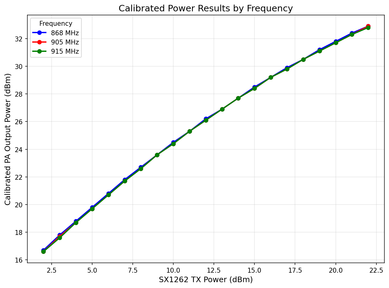
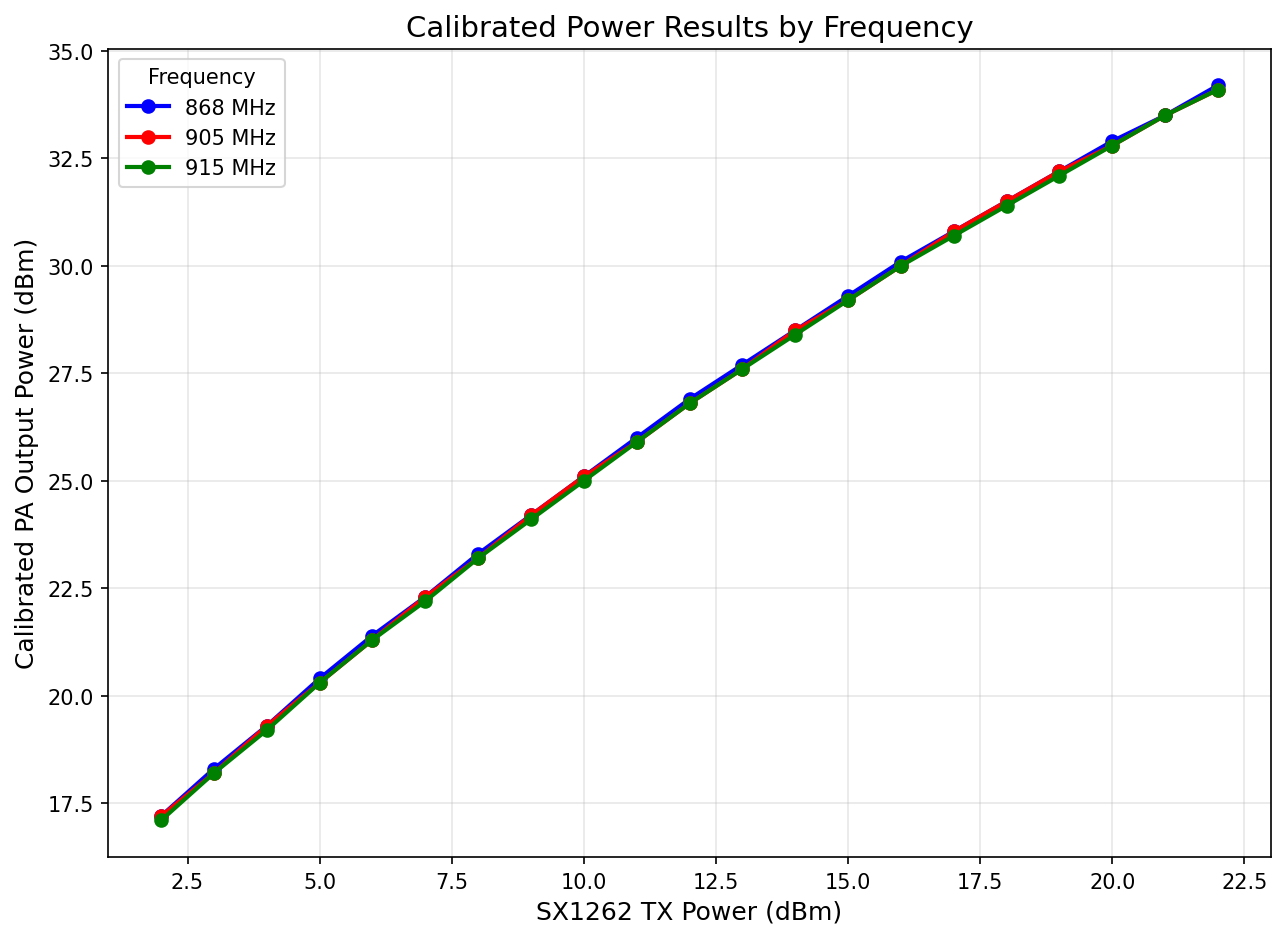
¶ Lora Power Amplifier Conduction Test for RF daughterboard - BQ35LORA900V1M
Based on the PA Operating Mode configuration, select the corresponding Power Level tab below. For the vast majority of firmware, unless otherwise specified. The "SX1262 TX Power Setting" refers to the LoRa TX power configured in the firmware or software, this can be understood as the input power to the LoRa Power Amplifier. The "PA Output Power" represents the power output to the antenna.
Test Conditions: BW 125 kHz, SF 12, CR 4/5, Sync 0xFF, transmitting 150 characters.
| SX1262 TX Power Setting (dBm) | PA Output Power (dBm) - 868MHz | PA Output Power (dBm) - 905MHz | PA Output Power (dBm) - 915MHz | Description |
|---|---|---|---|---|
| 2 | 16.7 | 16.6 | 16.6 | |
| 3 | 17.8 | 17.7 | 17.6 | |
| 4 | 18.8 | 18.7 | 18.7 | |
| 5 | 19.8 | 19.7 | 19.7 | |
| 6 | 20.8 | 20.7 | 20.7 | |
| 7 | 21.8 | 21.7 | 21.7 | |
| 8 | 22.7 | 22.6 | 22.6 | |
| 9 | 23.6 | 23.6 | 23.6 | |
| 10 | 24.5 | 24.4 | 24.4 | |
| 11 | 25.3 | 25.3 | 25.3 | |
| 12 | 26.2 | 26.1 | 26.1 | |
| 13 | 26.9 | 26.9 | 26.9 | Operation with ISM band for EU868 |
| 14 | 27.7 | 27.7 | 27.7 | |
| 15 | 28.5 | 28.4 | 28.4 | |
| 16 | 29.2 | 29.2 | 29.2 | |
| 17 | 29.9 | 29.8 | 29.8 | |
| 18 | 30.5 | 30.5 | 30.5 | Operation with ISM band for US915 |
| 19 | 31.2 | 31.1 | 31.1 | Mestastic Station G2 firmware limitation |
| 20 | 31.8 | 31.7 | 31.7 | |
| 21 | 32.4 | 32.3 | 32.3 | |
| 22 | 32.9 | 32.9 | 32.8 |
Caution!
All measurements above are indicative and typical, and are not a specification. The RF output power accuracy of the BQ35LORA900V1M daughterboard cannot be claimed to be better than the RF output power step accuracy of Semtech LoRa transceiver SX1262. Although the statistical accuracy of the BQ35LORA900V1M's PA Output Power is +-1dBm based on the conduction test in quality inspection, we still cannot guarantee that the batch-to-batch tolerance of the SX1262 will not change in the future.
According to the datasheet of SX1262, table 3-9: Transmit Mode Specifications, on the page 21. The RF output power step accuracy of SX1262 is +-2 dB.
In summary, although the statistical accuracy of the BQ35LORA900V1M's PA Output Power is +-1dBm, the PA Output Power accuracy should still be claimed to be +-2 dBm to be consistent with SX1262.
Typical Power Consumption
| Hardware Configuration | PA Operating Mode | RX Power Consumption (W) | TX Power Consumption (W) |
|---|---|---|---|
| ESP32S3-BQ35LORA900V1M | Power Level 1 | 0.560 | 6.330 |
Note: The system's overall power consumption is dependent on the firmware, peripherals, and antenna SWR, the data provided above represents typical power consumption. In most mesh networks, the TX time is significantly shorter than the RX time, so the overall power consumption is typically dominated by RX power consumption. Since almost all power consumption in RX mode comes from the MCU daughterboard, power consumption of the MCU daughterboard is critical for low-power applications.
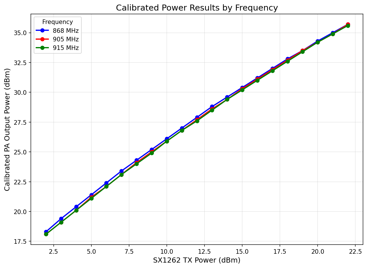
| SX1262 TX Power Setting (dBm) | PA Output Power (dBm) - 868MHz | PA Output Power (dBm) - 905MHz | PA Output Power (dBm) - 915MHz | Description |
|---|---|---|---|---|
| 2 | 17.2 | 17.2 | 17.1 | |
| 3 | 18.3 | 18.2 | 18.2 | |
| 4 | 19.3 | 19.3 | 19.2 | |
| 5 | 20.4 | 20.3 | 20.3 | |
| 6 | 21.4 | 21.3 | 21.3 | |
| 7 | 22.3 | 22.3 | 22.2 | |
| 8 | 23.3 | 23.2 | 23.2 | |
| 9 | 24.2 | 24.2 | 24.1 | |
| 10 | 25.1 | 25.1 | 25.0 | |
| 11 | 26.0 | 25.9 | 25.9 | |
| 12 | 26.9 | 26.8 | 26.8 | Operation with ISM band for EU868 |
| 13 | 27.7 | 27.6 | 27.6 | |
| 14 | 28.5 | 28.5 | 28.4 | |
| 15 | 29.3 | 29.2 | 29.2 | |
| 16 | 30.1 | 30.0 | 30.0 | Operation with ISM band for US915 |
| 17 | 30.8 | 30.8 | 30.7 | |
| 18 | 31.5 | 31.5 | 31.4 | |
| 19 | 32.2 | 32.2 | 32.1 | Mestastic Station G2 firmware limitation |
| 20 | 32.9 | 32.8 | 32.8 | |
| 21 | 33.5 | 33.5 | 33.5 | |
| 22 | 34.2 | 34.1 | 34.1 |
Caution!
All measurements above are indicative and typical, and are not a specification. The RF output power accuracy of the BQ35LORA900V1M daughterboard cannot be claimed to be better than the RF output power step accuracy of Semtech LoRa transceiver SX1262. Although the statistical accuracy of the BQ35LORA900V1M's PA Output Power is +-1dBm based on the conduction test in quality inspection, we still cannot guarantee that the batch-to-batch tolerance of the SX1262 will not change in the future.
According to the datasheet of SX1262, table 3-9: Transmit Mode Specifications, on the page 21. The RF output power step accuracy of SX1262 is +-2 dB.
In summary, although the statistical accuracy of the BQ35LORA900V1M's PA Output Power is +-1dBm, the PA Output Power accuracy should still be claimed to be +-2 dBm to be consistent with SX1262.
Typical Power Consumption
| Hardware Configuration | PA Operating Mode | RX Power Consumption (W) | TX Power Consumption (W) |
|---|---|---|---|
| ESP32S3-BQ35LORA900V1M | Power Level 2 | 0.510 | 7.510 |
Note: The system's overall power consumption is dependent on the firmware, peripherals, and antenna SWR, the data provided above represents typical power consumption. In most mesh networks, the TX time is significantly shorter than the RX time, so the overall power consumption is typically dominated by RX power consumption. Since almost all power consumption in RX mode comes from the MCU daughterboard, power consumption of the MCU daughterboard is critical for low-power applications.
| SX1262 TX Power Setting (dBm) | PA Output Power (dBm) - 868MHz | PA Output Power (dBm) - 905MHz | PA Output Power (dBm) - 915MHz | Description |
|---|---|---|---|---|
| 2 | 18.3 | 18.1 | 18.1 | |
| 3 | 19.4 | 19.1 | 19.1 | |
| 4 | 20.4 | 20.1 | 20.1 | |
| 5 | 21.4 | 21.2 | 21.1 | |
| 6 | 22.4 | 22.1 | 22.1 | |
| 7 | 23.4 | 23.1 | 23.1 | |
| 8 | 24.3 | 24.1 | 24.0 | |
| 9 | 25.2 | 25.0 | 24.9 | |
| 10 | 26.1 | 25.9 | 25.9 | |
| 11 | 27.0 | 26.8 | 26.8 | Operation with ISM band for EU868 |
| 12 | 27.9 | 27.7 | 27.6 | |
| 13 | 28.8 | 28.6 | 28.5 | |
| 14 | 29.6 | 29.4 | 29.4 | |
| 15 | 30.4 | 30.3 | 30.2 | Operation with ISM band for US915 |
| 16 | 31.2 | 31.1 | 31.0 | |
| 17 | 32.0 | 31.9 | 31.8 | |
| 18 | 32.8 | 32.7 | 32.6 | |
| 19 | 33.5 | 33.5 | 33.4 | Mestastic Station G2 firmware limitation |
| 20 | 34.3 | 34.2 | 34.2 | |
| 21 | 35.0 | 34.9 | 34.9 | |
| 22 | 35.7 | 35.7 | 35.6 |
Caution!
All measurements above are indicative and typical, and are not a specification. The RF output power accuracy of the BQ35LORA900V1M daughterboard cannot be claimed to be better than the RF output power step accuracy of Semtech LoRa transceiver SX1262. Although the statistical accuracy of the BQ35LORA900V1M's PA Output Power is +-1dBm based on the conduction test in quality inspection, we still cannot guarantee that the batch-to-batch tolerance of the SX1262 will not change in the future.
According to the datasheet of SX1262, table 3-9: Transmit Mode Specifications, on the page 21. The RF output power step accuracy of SX1262 is +-2 dB.
In summary, although the statistical accuracy of the BQ35LORA900V1M's PA Output Power is +-1dBm, the PA Output Power accuracy should still be claimed to be +-2 dBm to be consistent with SX1262.
Typical Power Consumption
| Hardware Configuration | PA Operating Mode | RX Power Consumption (W) | TX Power Consumption (W) |
|---|---|---|---|
| ESP32S3-BQ35LORA900V1M | Power Level 3 | 0.500 | 9.580 |
Note: The system's overall power consumption is dependent on the firmware, peripherals, and antenna SWR, the data provided above represents typical power consumption. In most mesh networks, the TX time is significantly shorter than the RX time, so the overall power consumption is typically dominated by RX power consumption. Since almost all power consumption in RX mode comes from the MCU daughterboard, power consumption of the MCU daughterboard is critical for low-power applications.
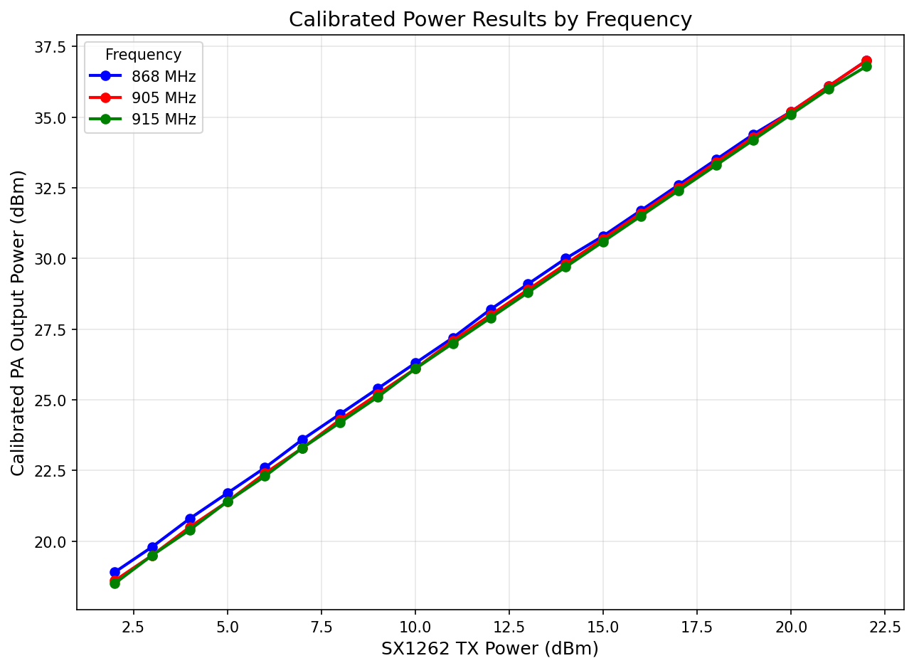
| SX1262 TX Power Setting (dBm) | PA Output Power (dBm) - 868MHz | PA Output Power (dBm) - 905MHz | PA Output Power (dBm) - 915MHz | Description |
|---|---|---|---|---|
| 2 | 18.9 | 18.6 | 18.5 | |
| 3 | 19.8 | 19.5 | 19.5 | |
| 4 | 20.8 | 20.5 | 20.4 | |
| 5 | 21.7 | 21.4 | 21.4 | |
| 6 | 22.6 | 22.4 | 22.3 | |
| 7 | 23.6 | 23.3 | 23.3 | |
| 8 | 24.5 | 24.3 | 24.2 | |
| 9 | 25.4 | 25.2 | 25.1 | |
| 10 | 26.3 | 26.1 | 26.1 | |
| 11 | 27.2 | 27.1 | 27.0 | Operation with ISM band for EU868 |
| 12 | 28.2 | 28.0 | 27.9 | |
| 13 | 29.1 | 28.9 | 28.8 | |
| 14 | 30.0 | 29.8 | 29.7 | Operation with ISM band for US915 |
| 15 | 30.8 | 30.7 | 30.6 | |
| 16 | 31.7 | 31.6 | 31.5 | |
| 17 | 32.6 | 32.5 | 32.4 | |
| 18 | 33.5 | 33.4 | 33.3 | |
| 19 | 34.4 | 34.3 | 34.2 | Mestastic Station G2 firmware limitation |
| 20 | 35.2 | 35.2 | 35.1 | |
| 21 | 36.1 | 36.1 | 36.0 | |
| 22 | 37.0 | 37.0 | 36.8 |
Caution!
All measurements above are indicative and typical, and are not a specification. The RF output power accuracy of the BQ35LORA900V1M daughterboard cannot be claimed to be better than the RF output power step accuracy of Semtech LoRa transceiver SX1262. Although the statistical accuracy of the BQ35LORA900V1M's PA Output Power is +-1dBm based on the conduction test in quality inspection, we still cannot guarantee that the batch-to-batch tolerance of the SX1262 will not change in the future.
According to the datasheet of SX1262, table 3-9: Transmit Mode Specifications, on the page 21. The RF output power step accuracy of SX1262 is +-2 dB.
In summary, although the statistical accuracy of the BQ35LORA900V1M's PA Output Power is +-1dBm, the PA Output Power accuracy should still be claimed to be +-2 dBm to be consistent with SX1262.
Typical Power Consumption
| Hardware Configuration | PA Operating Mode | RX Power Consumption (W) | TX Power Consumption (W) |
|---|---|---|---|
| ESP32S3-BQ35LORA900V1M | Power Level 4 | 0.550 | 11.270 |
Note: The system's overall power consumption is dependent on the firmware, peripherals, and antenna SWR, the data provided above represents typical power consumption. In most mesh networks, the TX time is significantly shorter than the RX time, so the overall power consumption is typically dominated by RX power consumption. Since almost all power consumption in RX mode comes from the MCU daughterboard, power consumption of the MCU daughterboard is critical for low-power applications.
¶ Primary Slot LNA Operating Mode Configuration Jumper LNA P
| LNA Operating Mode | LNA P | Description |
|---|---|---|
| LNA ON | OPEN | External LNA with dynamic gain control and impedance matching is enabled. When the environment noise floor is relatively low, RX sensitivity can be significantly enhanced, thereby increasing the RX coverage radius. |
| LNA OFF | SHORT | External LNA is disabled. When the environment noise floor is high, disabling the external LNA may help improve the SNR. |
Note: OPEN indicates that the 2.54mm jumper is NOT installed. SHORT indicates the 2.54mm jumper is installed.
Dynamic gain control, dynamic impedance matching, and LNA disable features enable the RF daughterboard—BQ35LORA900V1M to achieve better compatibility with high-gain monopole antennas in relatively high-noise environments compared to Station G2. The RX link design focuses on achieving an optimized RX dynamic range using active components alone, without employing passive filters. This design delivers approximately 5 dB of RX dynamic range improvement over the Station G2. When the LNA is disabled, it still offers roughly 3 dB of RX dynamic range improvement compared to the Nano series (which lacks an external LNA). Please note that real-world RX performance is heavily influenced by local terrain and propagation conditions.
Unlike passive filters, which are primarily limited to attenuating out-of-band interference, RX dynamic range optimization enables the suppression of both in-band and out-of-band noise. In complex electromagnetic environments, incorporating a cavity filter can further optimize RX performance by handling strong out-of-band signals, thereby allowing the system's dynamic range optimization to focus more effectively on mitigating in-band noise.
¶ Step 3 – Power the Device
WARNING: OPERATION WITHOUT AN ANTENNA MAY PERMANENTLY DAMAGE THE DEVICE.
WARNING: OPERATE ON AN INSULATED SURFACE. ENSURE PROPER INSULATION DURING OPERATION.
WHETHER USING A 15VDC USB TYPE-C PD ADAPTER OR A 9VDC–19VDC EXTERNAL POWER SUPPLY, THE MAXIMUM PEAK INPUT VOLTAGE TO THE STATION G3 MUST NOT EXCEED 19V. OTHERWISE, THE DEVICE MAY BE PERMANENTLY DAMAGED.
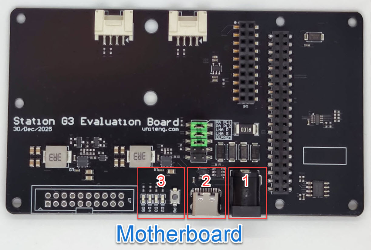
| No. | Description |
|---|---|
| 1 | DC5521 Socket (Positive inside, Negative outside, with the reverse polarity protection diode.) |
| 2 | USB Type C Socket |
| 3 | Power Good Checker |
The Station G3 can be powered by either 15VDC USB Type C PD protocol or 9VDC-19VDC Power Supply with a minimum power rating of 25 W via DC5521 Socket. A Power Supply with an input voltage range of 10–19 VDC and a rated power output of at least 25 W is required, when operating at PA Power Level 4.
Caution!
Our official MCU daughterboard can only be powered using the motherboard via Raspberry Pi compatible 40-pin GPIO connector, the USB Type-C port on the MCU daughterboard only provides communication function and cannot be used for power supply. Based on this design, our MCU daughterboard allows users to connect to a computer via the USB Type-C port on the daughterboard, while it is being powered by the motherboard.
For third-party daughterboards, such as the Raspberry Pi. We do not recommend connecting them to a computer via their own USB ports after they have been installed on the Station G3 Motherboard and powered by the Station G3 Motherboard, as we cannot verify whether these designs have reverse polarity protection or reverse current prevention mechanisms. Please note that the Ethernet interface can be considered safe for connection due to the built-in isolation transformer.
¶ Power Good Checker
When the PG button is pressed, a properly functioning power supply will enable the corresponding LED. All LEDs must be enabled simultaneously for the Station G3 to meet its operating conditions.
| LED ON | Description |
|---|---|
| D2 | The 3.3V LDO/DCDC on the MCU daughterboard is functioning normally. |
| D3 | The 3.3V LDO on the Motherboard for GROVE I2C and GROVE GPS Sockets is functioning normally. |
| D4 | The 5.0V DCDC on the Motherboard is functioning normally. |
| D5 | Fast-Transient DC-DC for LoRa Power Amplifier is functioning normally. |
¶ Step 4 – Install/Upgrade Firmware
WARNING: OPERATION WITHOUT AN ANTENNA MAY PERMANENTLY DAMAGE THE DEVICE.
If the device does not come with the desired firmware, or if you wish to upgrade to the latest version, please refer to this section to install or upgrade the firmware. Otherwise, you may skip this section.
¶ Order Option - ESP32S3-BQ35LORA900V1M
The Station G3 - ESP32S3-BQ35LORA900V1M is fully compatible with the Station G2 firmwares. Therefore, we can directly use the Station G2 firmwares.
You may need to manually set Station G3 - ESP32S3-BQ35LORA900V1M to enter the Firmware Download mode.
1.Please install the antenna before powering on the Station G3.
2.Connect the MCU daughterboard to the computer using a USB cable. Simultaneously, the motherboard must also be powered by either 15VDC USB Type C PD protocol or 9VDC-19VDC Power Supply with a minimum power rating of 25 W via DC5521 Socket.
3.Press and hold Firmware Download Button
4.Then single press Restart Button
5.Wait for 5 seconds ( For Windows, you may hear a sound when the USB device is reconnected automatically )
6.Finally release the Firmware Download Button
The device is now forced into Firmware Download mode
Note: After the flashing process is complete, you may need to single press Restart Button if the device does not reboot automatically.
¶ Meshtastic
Meshtastic Mesh Device Station G2 had been supported by the official meshtastic repository on Github from firmware version 2.2.24. Thus, the latest firmware could be downloaded from the meshtastic project’s releases page: https://github.com/meshtastic/Meshtastic-device/releases
Firmware file: firmware-station-g2-2.x.x.bin
Following instructions to flash it to the Station G2: https://meshtastic.org/docs/getting-started/flashing-firmware/esp32/
¶ Pull Requests related to Station G2
| Pull Request | Date | Github URL | Description |
|---|---|---|---|
| #3282 | 25-Feb-2024 | Station G2 #3282 | Initial Support for Station G2 |
¶ Meshcore
Please visit https://meshcore.io/flasher, select UnitEng Station G2, and follow the instructions on the Meshcore Web Flasher.
¶ Step 5 – Radio Configuration
¶ Meshtastic
Following the meshtastic official instructions to configure the radio.
https://meshtastic.org/docs/getting-started/initial-config/
¶ Meshcore
Following the meshcore official instructions to configure the radio.
https://docs.meshcore.io/faq/#1-introduction
¶ Advanced Topics
These advanced features are intended for experienced users and do not include official support coverage. While we cannot provide direct assistance, relevant communities often share useful information:
1. Our official Discord for hardware related topics: https://discord.gg/r9nEtXN6uB
2. Meshtastic: https://discord.gg/meshtastic
3. Meshcore: https://meshcore.gg/
WARNING: HARDWARE MODIFICATIONS OR THE USE OF UNVERIFIED THIRD-PARTY DAUGHTERBOARDS MAY CAUSE ELECTRICAL DAMAGE, COMPROMISE RF PERFORMANCE, OR RESULT IN FIRMWARE INCOMPATIBILITY. ALL HARDWARE CUSTOMIZATIONS ARE PERFORMED AT YOUR OWN RISK. THE MANUFACTURER ASSUMES NO LIABILITY FOR ANY DAMAGES OR ISSUES ARISING FROM USER-INITIATED MODIFICATIONS, AND USERS SHALL BEAR FULL RESPONSIBILITY FOR ALL OUTCOMES.
¶ Pinout
The Station G3 motherboard features a standard Raspberry Pi 40-pin GPIO header, designed to facilitate compatibility with a wide range of third-party MCU daughterboards and custom development modules. This modular architecture allows experienced engineers to integrate their own custom MCUs or Linux-capable boards (e.g., Raspberry Pi Zero 2W) to tailor the device for specific mesh networking applications.
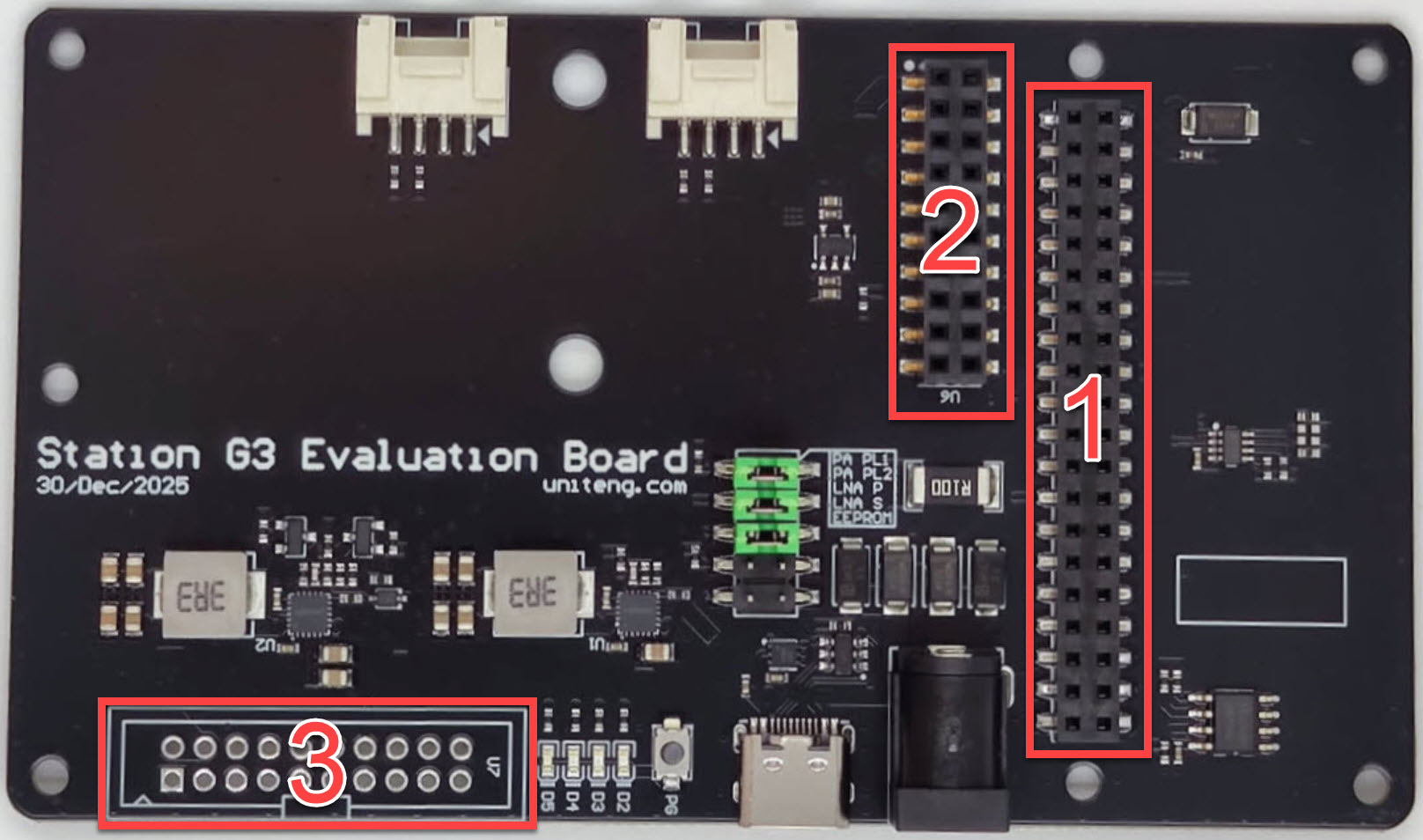
| Socket No. | Name | Description |
|---|---|---|
| 1 | MCU Daughterboard Socket | Raspberry Pi compatible 40-pin GPIO |
| 2 | Primary Slot for RF Daughterboard | The RF daughterboard is installed in this slot by default |
| 3 | Secondary Slot for RF Daughterboard | The socket is not soldered by default |
¶ Supported MCU Daughterboards
The following table lists the tested and verified boards for the MCU Daughterboard Socket (Socket No. 1). You can access the interactive pinout diagrams below to view specific pin functions by hovering over them:
| Board Name | Type | Interactive Pinout |
|---|---|---|
| BQESP32V1M | Official ESP32 S3 | View Diagram |
| Raspberry Pi Zero 2W | Third-party | View Diagram |
¶ Station G3 as Linux-Native Device
For third-party daughterboards, such as the Raspberry Pi. We do not recommend connecting them to a computer via their own USB ports after they have been installed on the Station G3 Motherboard and powered by the Station G3 Motherboard, as we cannot verify whether these designs have reverse polarity protection or reverse current prevention mechanisms. Please note that the Ethernet interface can be considered safe for connection due to the built-in isolation transformer.
THIRD-PARTY MCU DAUGHTERBOARDS MAY EXPERIENCE FALSE OVER-VOLTAGE TRIPPING AT HIGH RF POWER LEVELS. Some third-party boards utilize high-input-impedance operational amplifiers for power management voltage sampling. When the RF output power exceeds approximately 2W (an empirical value that varies depending on the specific design of the third-party board), near-field coupling can falsely trigger the over-voltage protection circuitry. While this typically does not cause permanent hardware damage, it may result in sudden system shutdowns that require a complete power cycle to recover. To prevent this, it is strongly recommended to install at least 0.5 meters of coaxial cable between the Station G3 SMA port and the antenna. This increases the physical distance between the antenna and the MCU daughterboard, effectively mitigating near-field interference and preventing false protection triggers.
Experienced users can also utilize the mPWRD-OS project (Armbian + Meshtastic), which supports a wider range of Linux development boards as MCU daughterboards, such as the Luckfox Lyra Zero W. For more details, visit: mPWRD-OS on GitHub.
¶ Hardware Installation
If the currently installed MCU daughterboard is not a Raspberry Pi Zero 2W, it must be replaced before proceeding. Follow these steps to safely swap the module:
- Remove the three or four M2.5 screws securing the corners of the existing MCU daughterboard, depending on the specific model in use.
- Carefully lift and remove the daughterboard from the socket. Avoid applying excessive force or prying to prevent damage to the SMT connector pins.
- Align the Raspberry Pi Zero 2W with the 40-pin GPIO header and secure it in place, as illustrated in the reference image above. Please ensure the antenna is installed before powering on the device via the USB Type C Socket or DC5521 Socket on the motherboard.
¶ Meshtastic
Note: The
meshtasticdproject iterates rapidly. Please always refer to the latest official documentation for the most up-to-date installation and usage instructions.
¶ Manual Installation of meshtasticd
To operate the Station G3 as a Linux-native Meshtastic node using the Raspberry Pi Zero 2W, follow the steps below:
- Interface Configuration: Enable SPI, I2C, and UART support on your Raspberry Pi Zero 2W. Detailed setup instructions are available in the official documentation: Raspberry Pi Hardware Setup.
- Install meshtasticd: On your Raspbian OS, install the
meshtasticdservice by following the official installation guide: Meshtasticd Installation. - Configure meshtasticd: Apply the
meshtasticdconfiguration file (.yaml) provided below. This configuration defines the specific hardware parameters for the Station G3 motherboard, along with essential software feature settings required for optimal mesh networking performance. For detailed usage instructions, refer to: Meshtasticd Usage Guide.
Lora:
  # File Name: lora-BQ-SG3-BQ35LORA900V1M-PrimarySlot.yaml
  # Board Doc: https://wiki.bqvoy.com/en/devkits/station-g3
  # Note: Device paths (spidev, I2CDevice) may differ across various operating systems and environments. Please verify these values for your specific setup.

  Module: sx1262
  IRQ: 22
  Reset: 16
  Busy: 24
  DIO3_TCXO_VOLTAGE: true
  DIO2_AS_RF_SWITCH: true
  spidev: spidev0.0
  #CS: 8

# Optional: I2C configuration (e.g., for external sensors or displays)
I2C:
  I2CDevice: /dev/i2c-1

# Optional: Advanced configuration parameters
Config:
  INA219_MULTIPLIER: 1.0f

# Optional: Webserver & Webservices settings
Webserver:
  Port: 443 # Port for Webserver & Webservices
  RootPath: /usr/share/meshtasticd/web # Root Dir of WebServer
Note: If you encounter initialization failures or RF communication errors, please verify your Raspberry Pi system configuration and runtime GPIO states:
- Ensure the following parameters are enabled in
/boot/firmware/config.txt:dtparam=i2c_arm=on dtoverlay=spi0-1cs dtoverlay=spi1-1cs- Run
pinctrl get 7-25in the terminal to verify peripheral initialization. The output for GPIO 8–11 must exactly match the following to satisfy the Primary Slot requirements:neil@LoraTesting:~ $ pinctrl get 7-25 7: ip -- | hi // GPIO7 = input 8: op -- -- | hi // GPIO8 = output 9: a0 -- | lo // GPIO9 = SPI0_MISO 10: a0 -- | lo // GPIO10 = SPI0_MOSI 11: a0 -- | lo // GPIO11 = SPI0_SCLK 12: ip -- | lo // GPIO12 = input 13: ip -- | lo // GPIO13 = input 14: ip -- | lo // GPIO14 = input 15: ip -- | hi // GPIO15 = input 16: ip -- | lo // GPIO16 = input 17: ip -- | hi // GPIO17 = input 18: op -- -- | hi // GPIO18 = output 19: a4 -- | lo // GPIO19 = SPI1_MISO 20: a4 -- | lo // GPIO20 = SPI1_MOSI 21: a4 -- | lo // GPIO21 = SPI1_SCLK 22: ip -- | lo // GPIO22 = input 23: ip -- | hi // GPIO23 = input 24: ip -- | lo // GPIO24 = input 25: ip -- | lo // GPIO25 = inputGPIO 18–21 are reserved for the Secondary Slot, which is typically unused in standard configurations.
¶ Utility Scripts
For advanced configurations and runtime control, the following shell scripts may be useful:
¶ lna_control.sh
Although the external LNA features dynamic gain control and impedance matching, its adjustable gain range is approximately 5 dB. In environments with high noise floors, the LNA may still become saturated. In such cases, disabling the LNA via software is a viable alternative to installing a cavity filter. For optimal RX performance, consider dynamically toggling the LNA state based on real-time noise floor measurements.
#!/bin/bash
# File Name: lna_control.sh
# Board Doc: https://wiki.bqvoy.com/en/devkits/station-g3
# Note: LNA Operating Mode Configuration for Primary Slot. Effective after removing Jumper LNA P.
# A high logic level is equivalent to installing Jumper LNA P, whereas a low logic level is equivalent to removing Jumper LNA P.

GPIO_CHIP="gpiochip0"
GPIO_PIN=23

case "$1" in
  LNAON)
    echo "LNA ON"
    gpioset ${GPIO_CHIP} ${GPIO_PIN}=0
    ;;

  LNAOFF)
    echo "LNA OFF"
    gpioset ${GPIO_CHIP} ${GPIO_PIN}=1
    ;;

  *)
    echo "Usage: $0 {LNAON|LNAOFF}"
    exit 1
    ;;
esac
¶ pa_control.sh
The Station G3 supports multiple Power Amplifier Operating Modes (Power Level 1 to 4), each exhibiting significantly different typical power consumption characteristics. For Station G3 nodes powered by batteries or solar energy, communicating with remote peers that have a sufficient link budget, switching to PA LOW LEVEL can save energy. Conversely, when communicating with remote nodes where the link budget is marginal, utilizing PA HIGH LEVEL ensures reliable packet delivery. Dynamically adjusting the Power Amplifier Operating Mode based on real-time mesh conditions and link quality is an effective strategy for optimizing battery life.
#!/bin/bash
# File Name: pa_control.sh
# Board Doc: https://wiki.bqvoy.com/en/devkits/station-g3
# Note: Power Amplifier Operating Mode Configuration. Effective after removing Jumper PA PL1.
# Based on the Jumper PA PL2 settings, configure Power Level 1/Power Level 3 or Power Level 2/Power Level 4.
# A high logic level is equivalent to installing Jumper PA PL1, whereas a low logic level is equivalent to removing Jumper PA PL1.

GPIO_CHIP="gpiochip0"
GPIO_PIN=17

case "$1" in
  PALOW)
    echo "PA LOW LEVEL"
    gpioset ${GPIO_CHIP} ${GPIO_PIN}=0
    ;;

  PAHIGH)
    echo "PA HIGH LEVEL"
    gpioset ${GPIO_CHIP} ${GPIO_PIN}=1
    ;;

  *)
    echo "Usage: $0 {PAON|PAOFF}"
    exit 1
    ;;
esac
¶ Troubleshooting
¶ Power Supply Verification
The electrical characteristics of the external power supply, specifically output impedance, ripple voltage, and load transient response, directly impact the Station G3’s RF performance and system stability .
Due to the significant current differential between RX and TX states, the power rail may experience instantaneous voltage droop during transmission. If the power supply lacks sufficient transient response capability or exhibits high output impedance, this rapid load step can cause the supply voltage to drop below critical thresholds. Additionally, excessive DC resistance in power cables or connectors will introduce a significant voltage drop under peak TX current, further exacerbating voltage drop. Such sudden voltage drop may trigger brownout conditions, resulting in system instability, RF front-end malfunction, or unexpected reboots.
To ensure reliable operation:
- Use a regulated power adapter compliant with the Station G3 specifications (10 VDC–19 VDC input, minimum 25 W rated output).
- Select a supply with low output impedance and tight ripple specifications (typically ≤150 mVpp lower is better).
- Ensure the power source supports fast transient response to accommodate peak TX current demands without significant voltage drop (typically ≤500 mVpp lower is better).
- Verify that all power cables and connectors exhibit minimal DC resistance to prevent additional voltage drop under load.
If you experience intermittent reboots or degraded RF performance, replacing the power adapter with a verified high-performance unit is often the most effective diagnostic step.
¶ Voltage Drop Measurement Using INA219
The Station G3 motherboard integrates an INA219 current/voltage sensor for real-time power rail monitoring. While the INA219’s sampling bandwidth is insufficient for high-frequency ripple analysis, it provides accurate measurements of DC voltage drop and current draw during RX-to-TX state transitions. For users operating the Station G3-ESP32S3-BQ35LORA900V1M, the following procedure utilizes a dedicated web-based diagnostic tool to evaluate power supply stability under peak load conditions.
- Hardware Setup: Install the antenna securely. Power the device via the motherboard’s DC5521 socket or USB Type-C PD port. Connect the USB Type-C port on the BQESP32V1M MCU daughterboard to your computer for serial communication.
- Flash Diagnostic Firmware: Open the Web Flasher at https://tools.bqvoy.com/stationg3/testing/flasher/?id=default and flash the Testing Firmware for Station G3 ESP32S3-BQ35LORA900V1M v1.0.
- Configure PA Operating Mode: Set the desired Power Amplifier Operating Mode using the
PA PL1andPA PL2jumpers on the motherboard, as specified in the hardware configuration section. - Run Voltage Drop Test: Navigate to the diagnostic web tool at https://tools.bqvoy.com/stationg3/testing/.
- Click Connect Device and select the COM port corresponding to your Station G3.
- In the Quick Actions panel, click Max TX Power, followed by Power Supply Check to initiate the test sequence.
- Upon completion, the interface will display real-time voltage/current summary metrics similar to the example below:
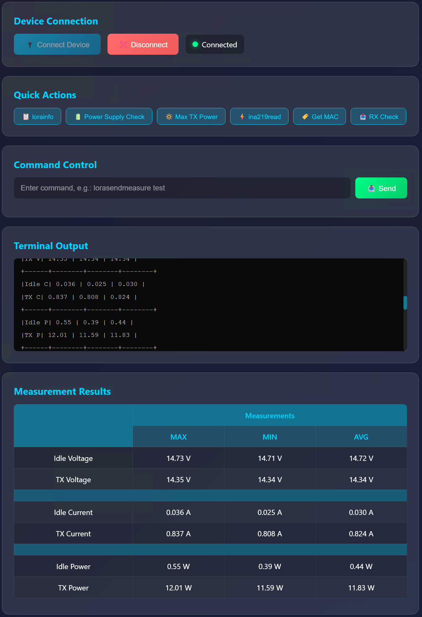
To evaluate power rail stability, calculate the voltage drop by comparing the Idle Voltage and TX Voltage readings. The difference in the AVG column should typically be ≤500 mVpp; lower values indicate superior transient response and reduced risk of brownout conditions.
Please note that both Idle and TX voltage readings will typically be approximately 0.5 V lower than the external power supply's output voltage. This offset occurs because the INA219 monitors the power rail downstream of the SS54 Schottky diode, which provides reverse-polarity protection. The forward voltage drop () across the SS54 is load-dependent and positively correlates with forward current. Under typical Station G3 operating conditions, this ranges from 0.45 V to 0.55 V.
Note: The INA219 is optimized for DC and low-frequency transient monitoring. For high-frequency ripple or fast edge transient analysis, an oscilloscope with appropriate probing techniques is recommended.